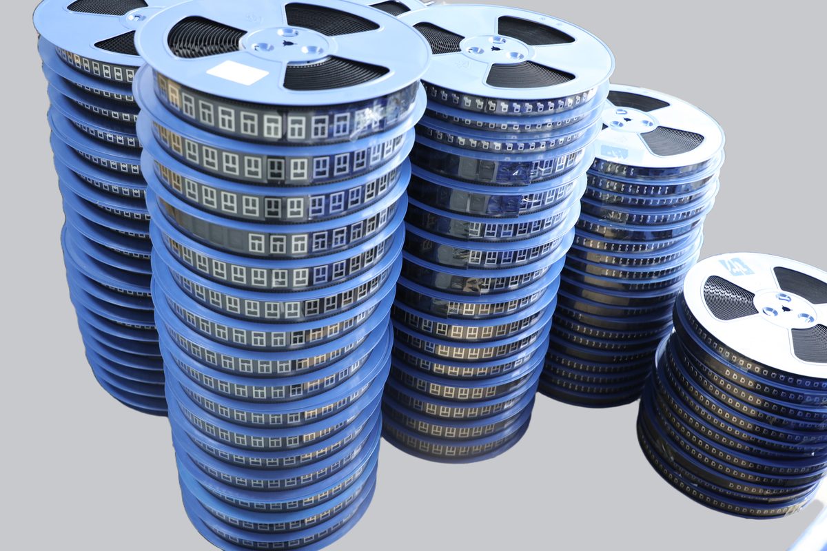
Covering one-piece, two-piece, frames, covers, clips, conductive gaskets, and all EMI shielding products. From 5×5mm micro shields to 80×80mm large custom sizes, meeting consumer electronics, 5G communications, and automotive electronics requirements.
From standard two-piece to custom multi-cavity solutions, each type is optimized for specific mounting methods, rework needs, and shielding performance.
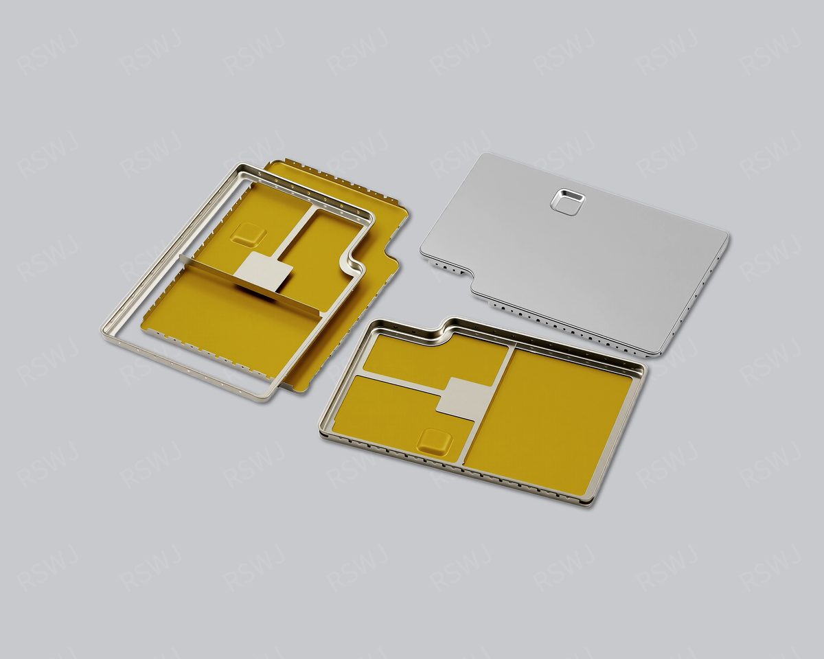
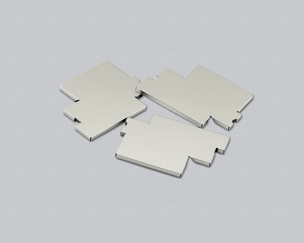
Industry-standard board-level shielding. Frame welded to PCB, snap-on cover for easy rework without desoldering.
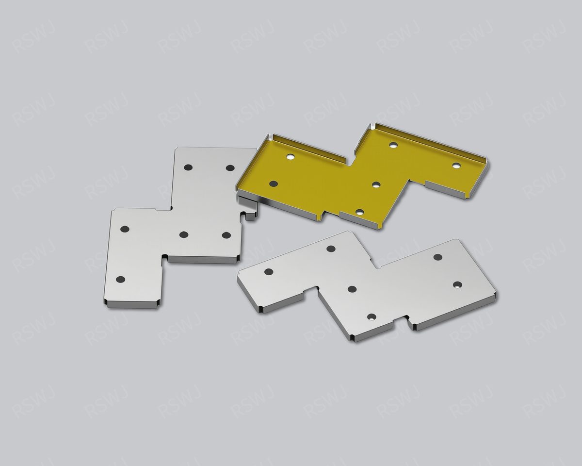
Deep-drawn seamless construction with no seams, maximum shielding efficiency. Ideal for space-constrained smartphones and wearables.
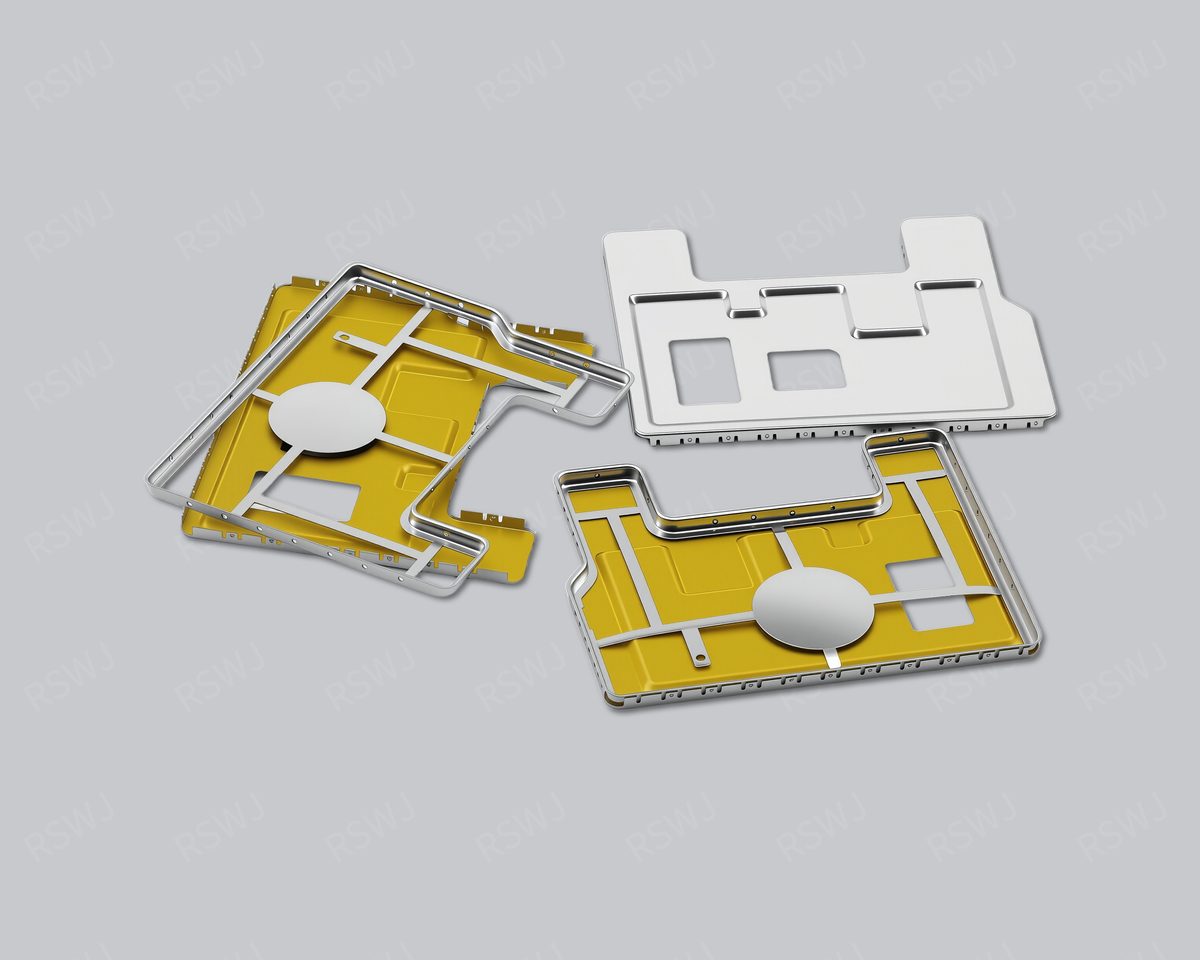
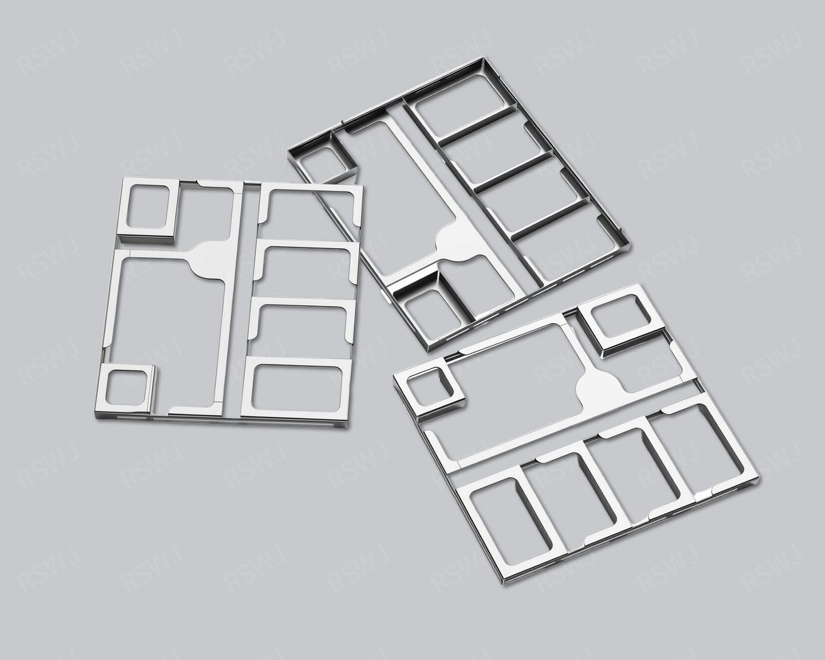
Precision-stamped frame welded to PCB for reliable grounding and shielding base. Supports multi-cavity compartment designs.
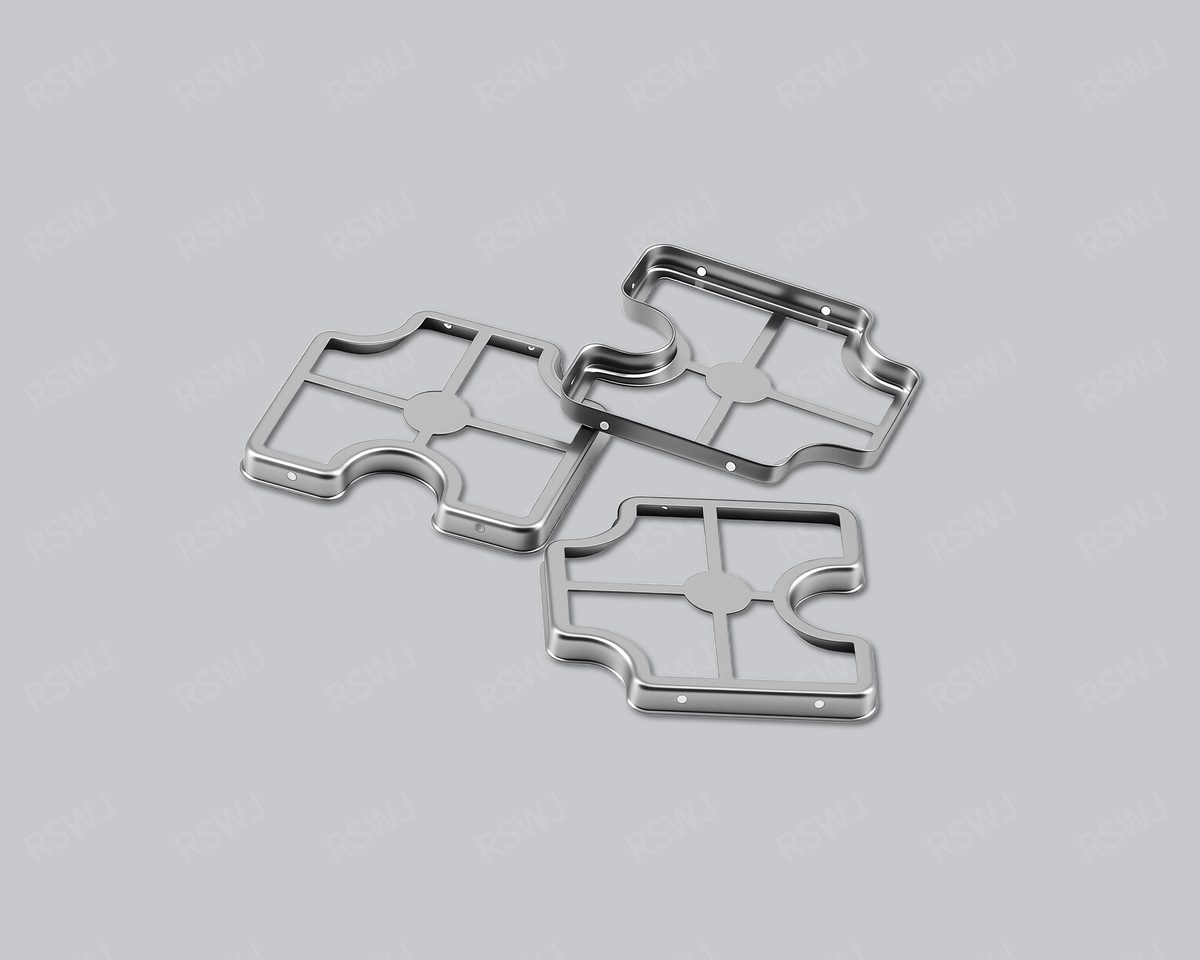
Snap-on/spring-clip covers with beryllium copper spring fingers. Reliable contact, quick assembly and disassembly for fast rework.
Beryllium copper/phosphor bronze spring fingers, precision-formed. Provide stable electrical contact and shielding continuity between can and PCB.
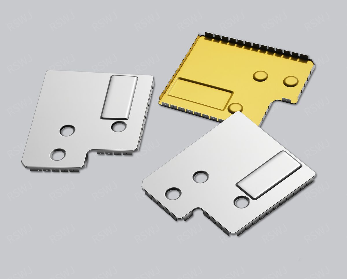
Internal partitions separate multiple RF circuit areas. For complex PCB layouts, isolate multiple regions with a single shielding enclosure.
Conductive silicone rubber, foam-backed fabric, metal-braided gaskets. Enhanced sealing and conductivity for high-level EMC requirements.
Provide drawings or requirements, our engineering team delivers full co-design support, DFM review, and rapid prototyping.
Different industries have different EMI shielding requirements—performance, certifications, and environmental factors. Choose your application domain for targeted solutions.
Smartphones/Tablets/TWS
Millimeter Wave/WiFi 6E/Bluetooth
ADAS/ECU/New Energy
Base Stations/Optical Modules/Routers
Medical Devices/Industrial Control/Servers
Smart Speakers/AI Accelerator Cards
Each material trades off shielding efficiency, weldability, corrosion resistance, and cost. Click to learn material properties and suitable applications.
Comprehensive comparison across cost, shielding efficiency, rework-ability, and height to select the best structure type.
Tin-plate, nickel silver, stainless steel, copper alloys—performance specs, applications, and cost comparison.
Dimension specs, PCB footprint, grounding design, aperture rules, height clearance—engineer design essentials.
Serving telecom, consumer electronics, automotive, medical and many other industries
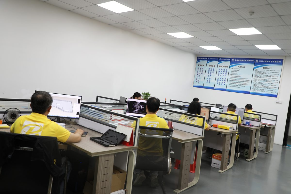
20+ high-precision stamping presses, 20-member professional R&D team, 2-3 day fast delivery, providing full-process service from design to mass production
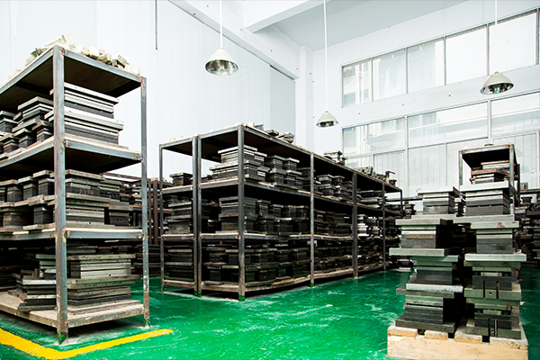
 Stamping Workshop
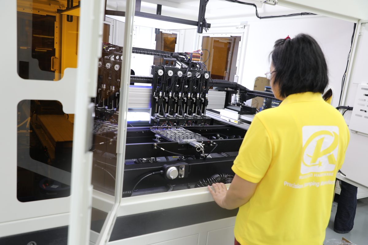
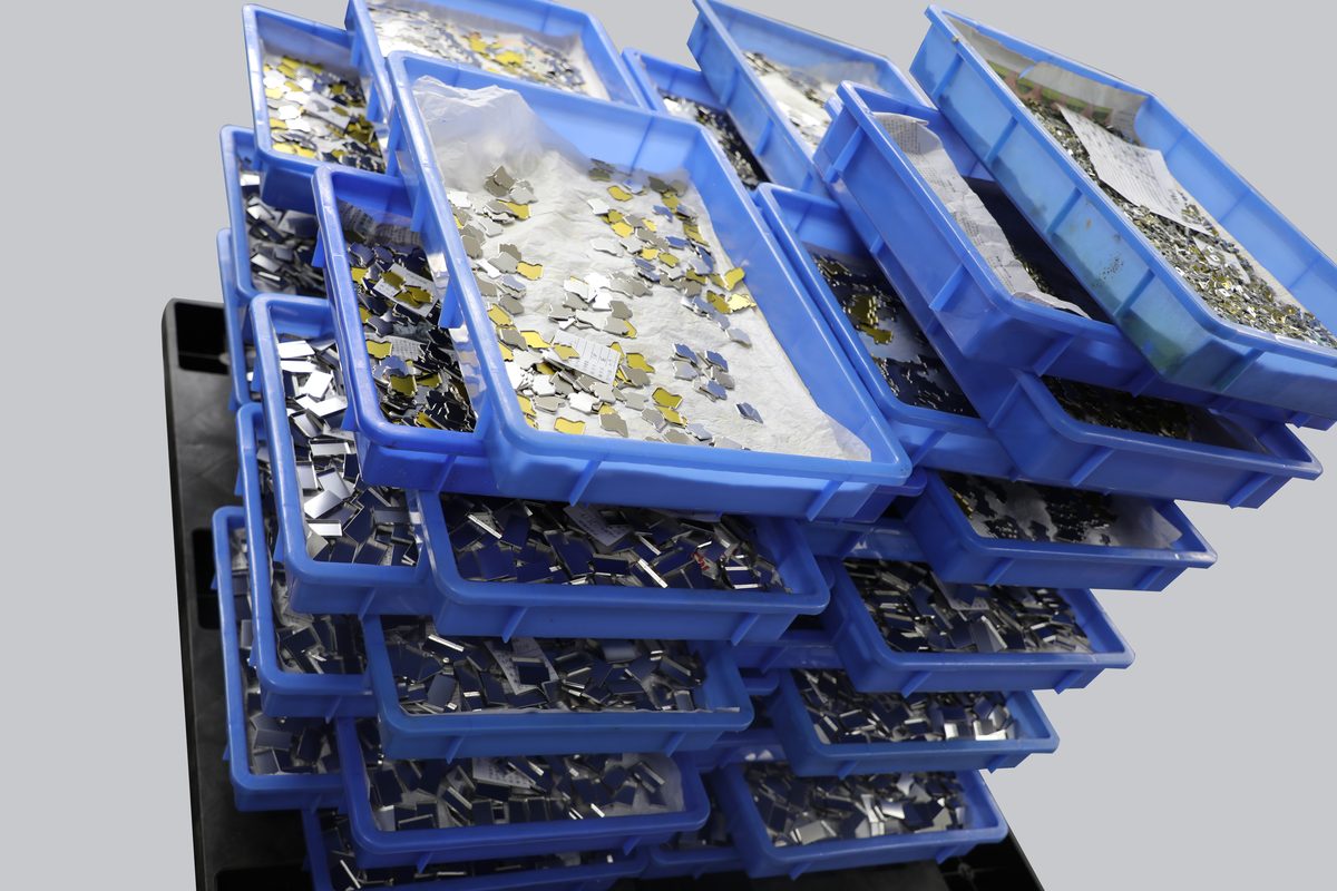
Equipped with 20+ high-speed precision stamping presses, with a daily stamping capacity of 3 million strokes and accuracy of ±0.01mm.
 Tooling Center
20-member professional R&D team, producing 100+ sets of precision tooling per month, from drawings to finished products in as fast as 2-3 days.
 Quality Lab
Incoming inspection → In-process control → Final inspection → Shipping inspection, dual certified with ISO 9001 and IATF 16949.
Over 90% of orders are custom products. Provide drawings or specifications, get a free quote with DFM recommendations within 24 hours.