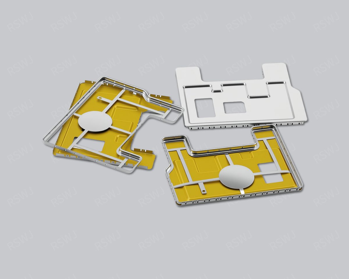
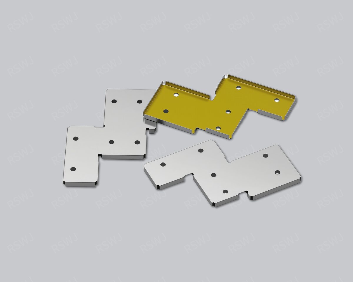
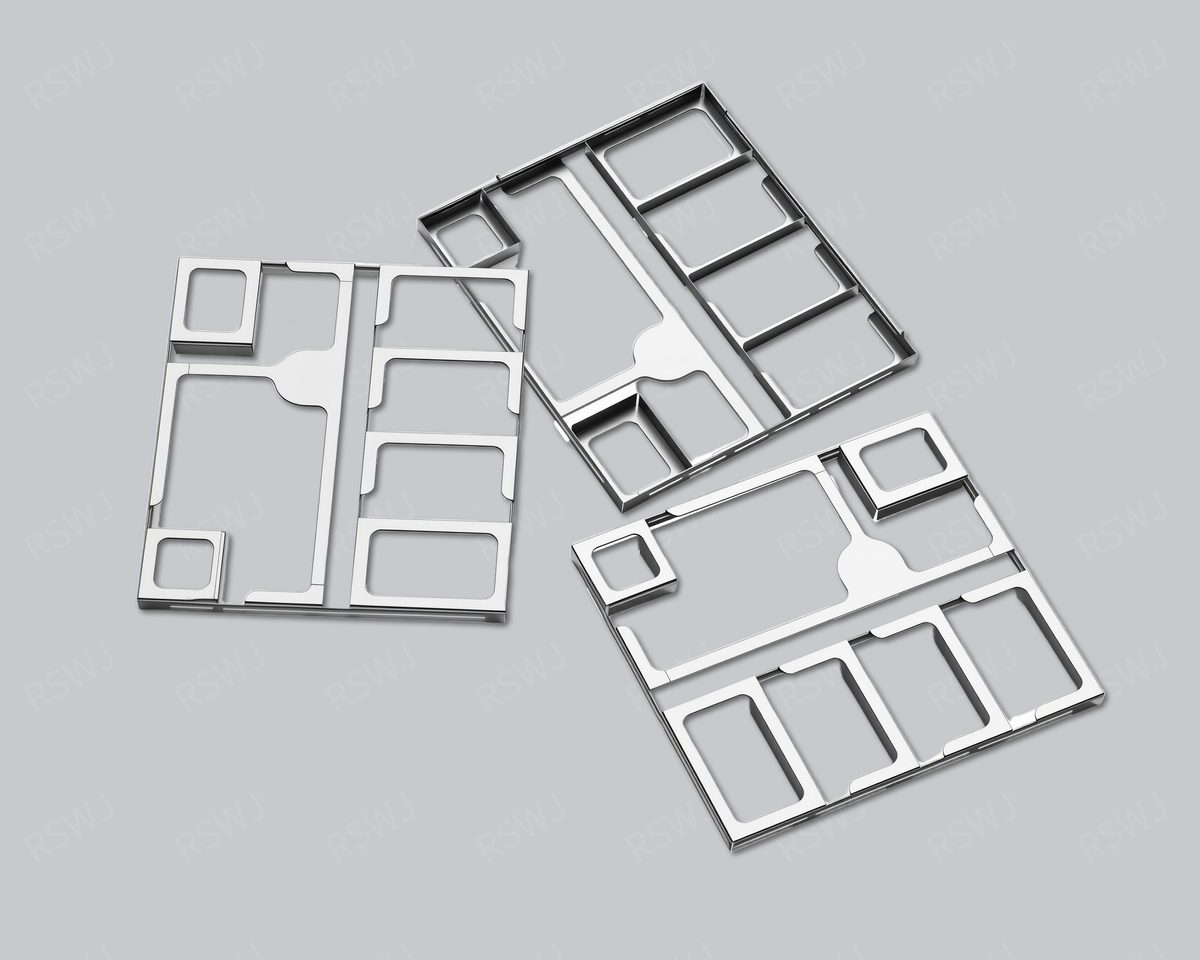
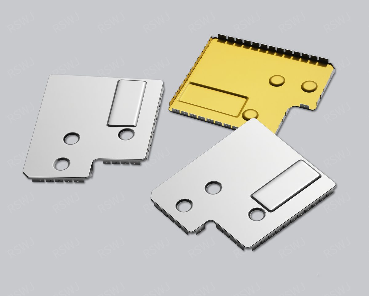
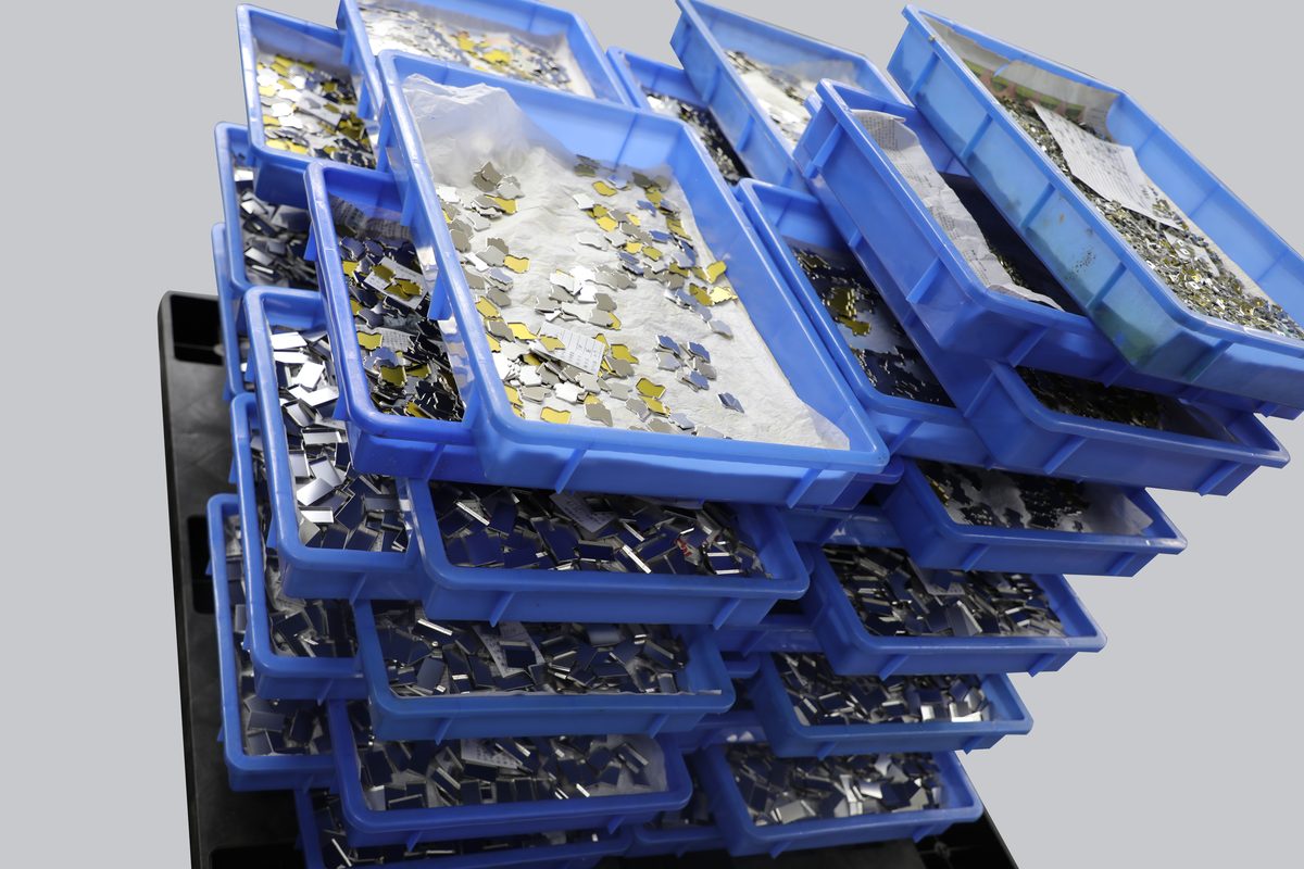
Precision stamped EMI shielding frame serving as the foundation component of two-piece shielding can solutions. Welded directly to PCB for reliable grounding and shielding foundation. Supports multi-cavity partition design, fully compatible with SMT processes. The core component of industry-standard board-level shielding.
Precision-designed PCB frame optimizing soldering performance, grounding efficiency, and multi-cavity flexibility.
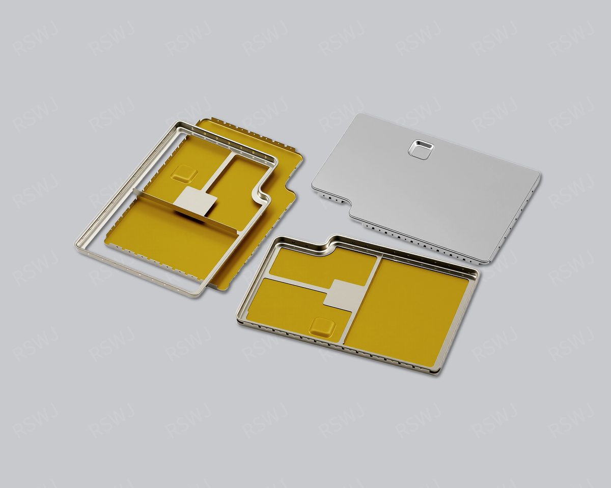
Uses high-precision stamping equipment to ensure frame flatness, squareness, and pad position accuracy, providing foundation for subsequent SMT soldering and cover installation.
Pad design follows IPC standards, fully compatible with all mainstream pick-and-place machines and reflow soldering processes, withstanding 260°C peak temperature.
Frame supports internal partitions or separators enabling multiple independent RF shielding regions within a single cover, accommodating complex circuit layouts.
Can freely design size, height, and partition positions based on PCB footprint and circuit layout for complete customization.
| Specification Item | Range and Description |
|---|---|
| Material Selection | Tin-plated steel (SPTE), Nickel silver, Stainless steel (SUS304), Copper, Brass, Aluminum alloy |
| Frame Format | Four-side frame, special shapes, multi-cavity partitions |
| Size Range | Minimum 5x5mm, Maximum 100x100mm, Custom sizes |
| Height Range | 2-15mm, customizable per application |
| Thickness Range | 0.15-0.3mm, multiple options |
| Tolerance Class | ±0.05mm (standard), ±0.02mm (precision) |
| Pad Design | Follows IPC standards, compatible with all SMT processes |
| Surface Treatment | Tin plating, Nickel plating, Gold plating, Plastic coating, Anodizing |
| Maximum Operating Temperature | -40°C to +120°C (reflow compatible 260°C) |
| Unit Weight | 0.5-50g (varies with size and material) |
Widely used in all electronic products requiring board-level EMI shielding.
RF module shielding for phones, tablets, and various consumer electronics.
5G base station equipment, WiFi 6E, and millimeter-wave communication module shielding.
EMI shielding for vehicle ECUs, ADAS, and OTA communication modules.
High-reliability EMI shielding design for medical instruments.
Electromagnetic protection for PLCs, frequency converters, and industrial control boards.
RF shielding foundation for various smart devices.
Serving telecom, consumer electronics, automotive, medical and many other industries
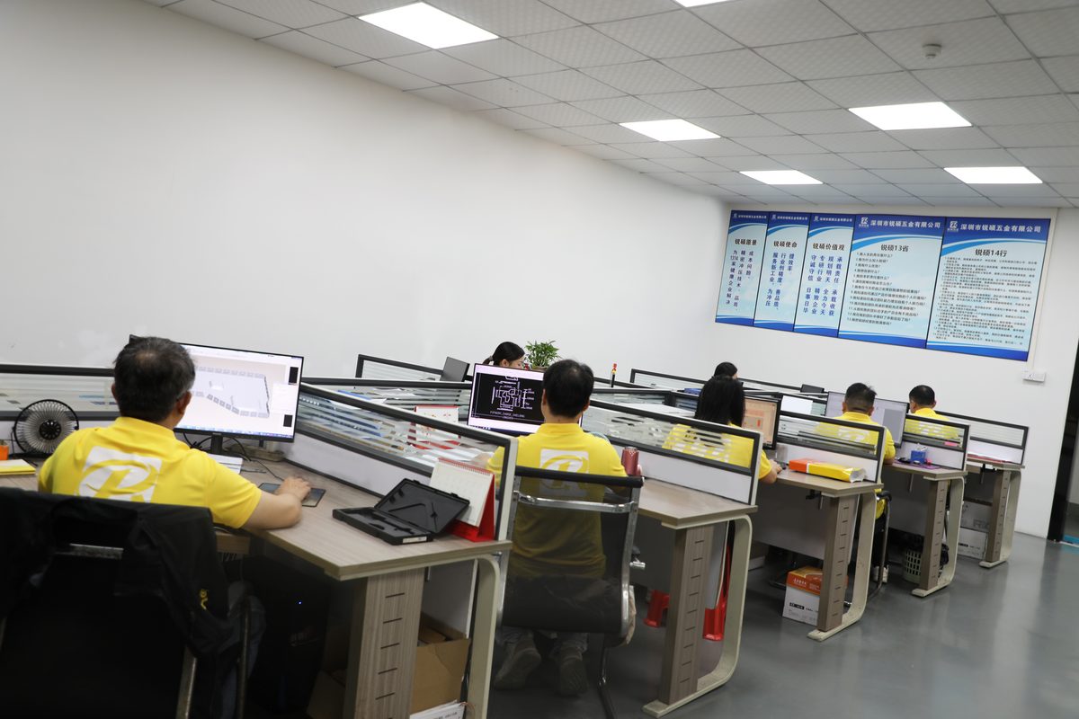
20+ high-precision stamping presses, 20-member professional R&D team, 2-3 day fast delivery, providing full-process service from design to mass production
 Stamping Workshop
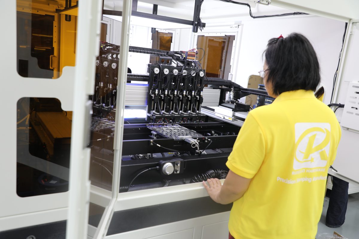
Equipped with 20+ high-speed precision stamping presses, with a daily stamping capacity of 3 million strokes and accuracy of ±0.01mm.
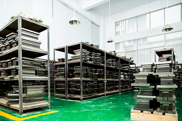
 Tooling Center
20-member professional R&D team, producing 100+ sets of precision tooling per month, from drawings to finished products in as fast as 2-3 days.
 Quality Lab
Incoming inspection → In-process control → Final inspection → Shipping inspection, dual certified with ISO 9001 and IATF 16949.
We can provide fully customized frame design and DFM review based on your PCB layout, circuit design, and performance requirements. Multi-cavity and special shapes supported.