Shenzhen Ruishuo Metal Co., Ltd. — ISO 9001 & IATF 16949 Certified
chinarswj@shieldingcover.com

IoT & AI Hardware Shielding Solutions

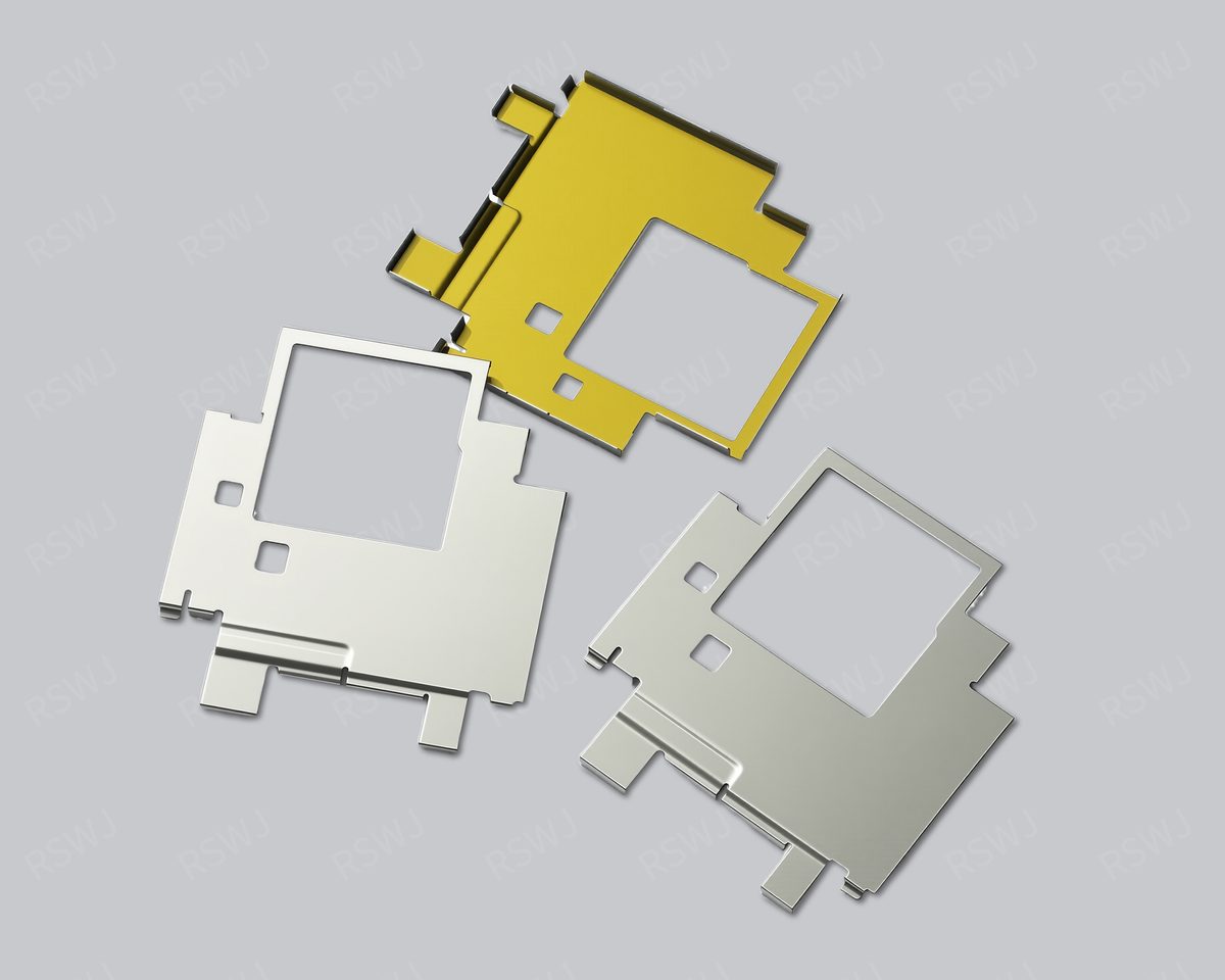
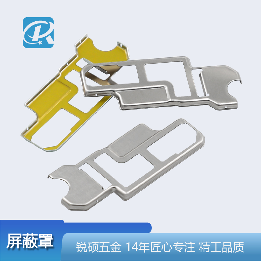
Compact, high-performance shielding cans for smart devices, AI accelerator cards, edge computing hardware. Multi-band support, thermal optimization, ultra-slim design—empowering next-generation intelligent hardware.

100+ IoT Projects
Multi-Band Optimized
Compact Design
Rapid Prototyping
Application Scenarios

IoT & AI Typical Applications

From smart home to edge computing, AI chips to IoT devices—covering intelligent-era core applications.

Smart Speakers

Multi-microphone array, WiFi/Bluetooth module, audio processing chip compact shielding. Low-height design preserving audio quality.

Smart Home Devices

Door locks, sensors, controllers and other home IoT device shielding solutions. Supporting Zigbee, Z-Wave, WiFi multi-protocol.

AI Accelerator Cards

GPU/TPU accelerator, inference card multi-module shielding solutions. High shielding efficiency, thermal optimization, multi-layer isolation.

Edge Computing Devices

Industrial edge computing gateways, industrial IoT controllers shielding. Supporting wide temperature range, multi-network protocols, high reliability.

Wearable Devices

Watch, bracelet, glasses and other wearable device ultra-compact shielding. Extreme size limits, low power, multi-sensor isolation.

Wireless Charging

Wireless charger, wireless power supply solution shielding. Protecting receiver circuits, avoiding power loss and interference.

Edge Computing

Edge Computing & AI Unique Requirements

15 Years+
EMI Shielding Manufacturing Experience
1300+
Global Clients
3M Strokes/Day
Daily Production Capacity
100+ Sets/Month
Tooling Development Capability
Trusted By

Chosen by Global Leading Brands

Serving telecom, consumer electronics, automotive, medical and many other industries

ISO 9001 Certified
IATF 16949 Certified
ISO 14001 Certified
NDA Signed
Manufacturing Strength

Professional EMI Shielding Cover Manufacturing Base

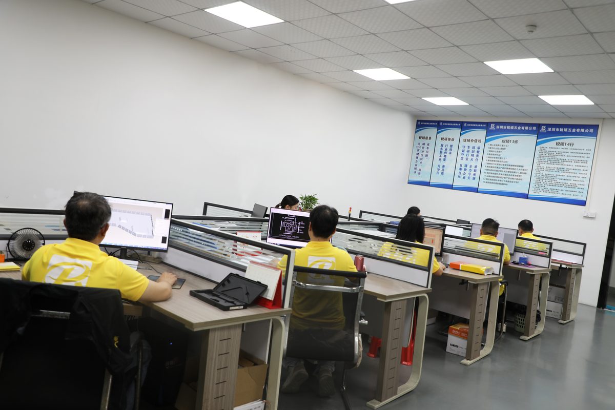
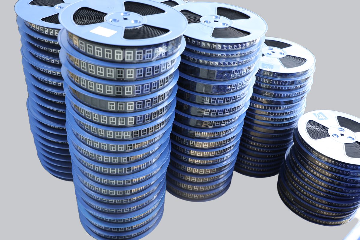
20+ high-precision stamping presses, 20-member professional R&D team, 2-3 day fast delivery, providing full-process service from design to mass production
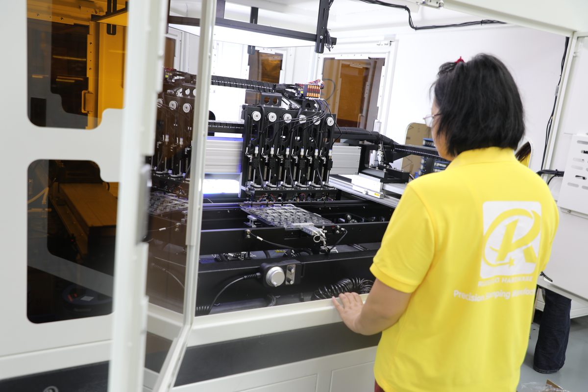
High-Precision Stamping Workshop Stamping Workshop

High-Precision Stamping Equipment

Equipped with 20+ high-speed precision stamping presses, with a daily stamping capacity of 3 million strokes and accuracy of ±0.01mm.

3M Strokes/Day ±0.01mm Precision
EMI Shielding Can Precision Stamping Manufacturing Tooling Center

In-House Tooling R&D Center

20-member professional R&D team, producing 100+ sets of precision tooling per month, from drawings to finished products in as fast as 2-3 days.

20 R&D Engineers 100+ Sets/Month
Quality Testing Laboratory Quality Lab

Full-Process Quality Control

Incoming inspection → In-process control → Final inspection → Shipping inspection, dual certified with ISO 9001 and IATF 16949.

ISO 9001 IATF 16949
IoT AI Solutions

Intelligent Device
Shielding Expert

We have provided shielding solutions for 50+ smart home brands, 30+ AI chip companies, and 20+ edge computing vendors. Whatever your product size or complexity, we find the optimal shielding solution.

Ultra-Compact Design
Multi-Band Optimized
Rapid Prototyping
Smart Device Shielding Can
IoT Project
EMI Shielding Can Precision Stamping Manufacturing
EMI Shielding Can Deep Drawing Manufacturing Process
FAQ

IoT AI Shielding Can Frequently Asked Questions

What precision can ultra-micro shielding cans (<5×5mm) achieve?

Our ultra-micro shielding can precision capability:

  • Dimensional Precision: ±0.02~±0.03mm, capable of 3×3mm or smaller applications;
  • Aperture Precision: 0.3mm apertures precise to ±0.05mm;
  • Thickness Precision: 0.3mm thickness controlled to ±0.03mm;
  • Consistency: Batch CV value <5%, guaranteeing large-volume use consistency.

We have specialized micro-stamping processes and precision inspection equipment—no dimensional concerns needed.

How is multi-band shielding designed without mutual interference?

Multi-Band Coordination Design Method:

  • Frequency Band Isolation: Multi-cavity frameworks or multi-layer shielding physically separate different-frequency circuits into different spaces;
  • Aperture Optimization: Optimize apertures for each band to avoid resonance and coupling;
  • Grounding Design: Multi-layer grounding ensuring complete inter-frequency isolation and grounding;
  • Simulation Verification: Use electromagnetic simulation tools (HFSS) predicting multi-band efficiency and optimizing design.

Key is early coordination of all frequency requirements—we coordinate optimal design.

How to balance AI accelerator card thermal management and shielding?

Thermal-Shielding Balance Solutions:

  • High-Thermal Materials: Copper or copper-alloy cans with 400+ W/mK thermal conductivity;
  • Thermal Pads: Bottom-surface thermal silicone pads (5 W/mK) directly contacting chips;
  • Ventilation Shielding: Top or side apertures with cooling fin or airway configurations;
  • Thermal Modeling: Thermal simulation (Fluent or Icepak) verifying chip temperatures meet operational requirements.

Typically achieves 50~70% thermal efficiency improvement with 10~20℃ chip temperature reduction.

How is wearable device shielding can bending and reliability assured?

Wearable device flexibility and reliability requirements:

  • Material Selection: High-elasticity alloys (such as phosphor copper) supporting bending deformation;
  • Structure Design: Flexible hinges or segmented frames allowing 360° bending;
  • Fatigue Testing: 10,000 bend cycle testing ensuring no fracture;
  • Contact Design: Elastic contact point design maintaining electrical connection during bending.

We have multiple mature wearable device shielding solutions ready for deployment.

How long does concept-to-production take?

Typical IoT Project Timeline:

  • Requirements Confirmation: 1 week confirming can size, bands, frequencies;
  • Design & Simulation: 2 weeks conducting electromagnetic and thermal simulation with DFM guidance;
  • Prototyping & Verification: 3 weeks including tool design, trial production, efficiency and reliability testing;
  • Sample Refinement: 2 weeks microadjusting solution based on test results;
  • Mass Production Prep: 2 weeks completing production process verification and first-article reports.

Total approximately 10 weeks (3 months) from concept to production-ready solution. Rush options available down to 8 weeks.